- 您现在的位置:买卖IC网 > Sheet目录342 > MCBSTM32EXL (Keil)BOARD EVALUATION FOR STM32F103ZE
�� �
�
�RM0008�
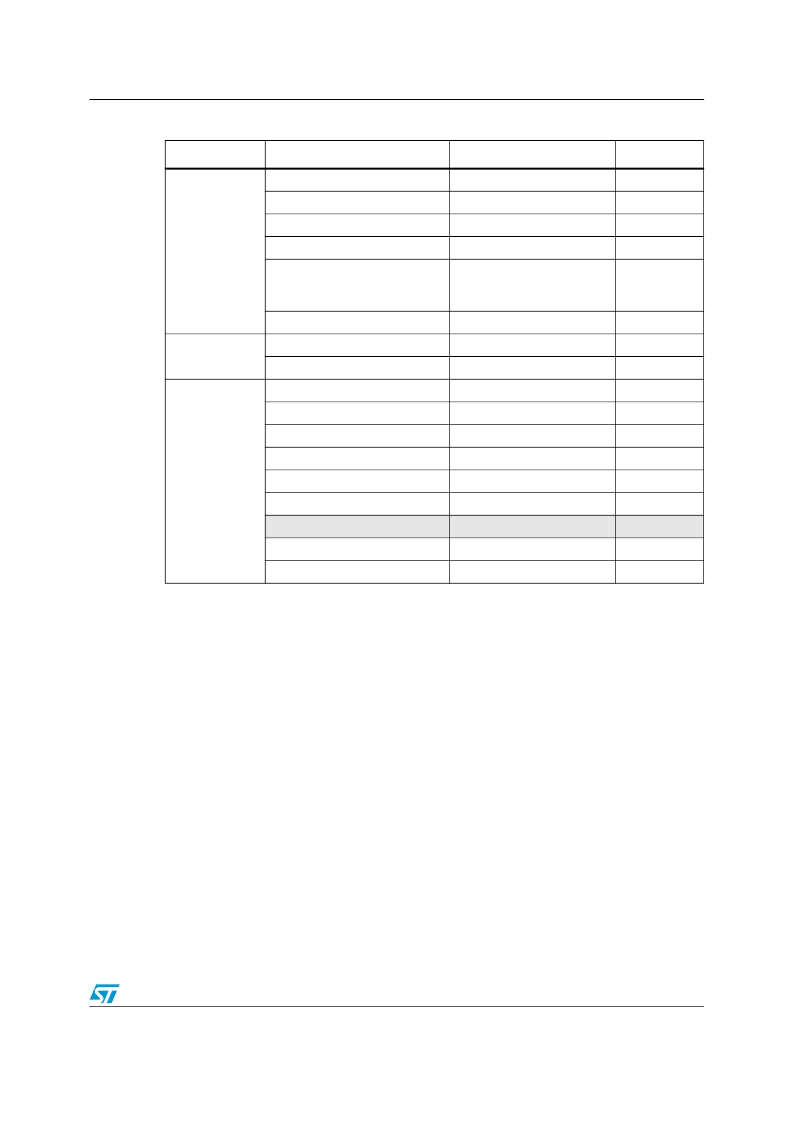
�Table� 5.�
�Memory� and� bus� architecture�
�Flash� module� organization� (connectivity� line� devices)�
�Block�
�Main� memory�
�Name�
�Page� 0�
�Page� 1�
�Page� 2�
�Page� 3�
�.�
�.�
�.�
�Page� 127�
�System� memory�
�Base� addresses�
�0x0800� 0000� -� 0x0800� 07FF�
�0x0800� 0800� -� 0x0800� 0FFF�
�0x0800� 1000� -� 0x0800� 17FF�
�0x0800� 1800� -� 0x0800� 1FFF�
�.�
�.�
�.�
�0x0803� F800� -� 0x0803� FFFF�
�0x1FFF� B000� -� 0x1FFF� F7FF�
�Size� (bytes)�
�2� Kbytes�
�2� Kbytes�
�2� Kbytes�
�2� Kbytes�
�.�
�.�
�.�
�2� Kbytes�
�18� Kbytes�
�Information� block�
�Option� Bytes�
�FLASH_ACR�
�FLASH_KEYR�
�FLASH_OPTKEYR�
�0x1FFF� F800� -� 0x1FFF� F80F�
�0x4002� 2000� -� 0x4002� 2003�
�0x4002� 2004� -� 0x4002� 2007�
�0x4002� 2008� -� 0x4002� 200B�
�16�
�4�
�4�
�4�
�Flash� memory�
�interface�
�registers�
�FLASH_SR�
�FLASH_CR�
�FLASH_AR�
�Reserved�
�FLASH_OBR�
�FLASH_WRPR�
�0x4002� 200C� -� 0x4002� 200F�
�0x4002� 2010� -� 0x4002� 2013�
�0x4002� 2014� -� 0x4002� 2017�
�0x4002� 2018� -� 0x4002� 201B�
�0x4002� 201C� -� 0x4002� 201F�
�0x4002� 2020� -� 0x4002� 2023�
�4�
�4�
�4�
�4�
�4�
�4�
�Note:�
�For� further� information� on� the� Flash� memory� interface� registers,� please� refer� to� the�
�STM32F10xxx� Flash� programming� manual.�
�Reading� the� Flash� memory�
�Flash� memory� instructions� and� data� access� are� performed� through� the� AHB� bus.� The�
�prefetch� block� is� used� for� instruction� fetches� through� the� ICode� bus.� Arbitration� is� performed�
�in� the� Flash� memory� interface,� and� priority� is� given� to� data� access� on� the� DCode� bus.�
�Read� accesses� can� be� performed� with� the� following� configuration� options:�
�●�
�●�
�●�
�Latency:� number� of� wait� states� for� a� read� operation� programmed� on-the-fly�
�Prefetch� buffer� (2� x� 64-bit� blocks):� it� is� enabled� after� reset;� a� whole� block� can� be�
�replaced� with� a� single� read� from� the� Flash� memory� as� the� size� of� the� block� matches� the�
�bandwidth� of� the� Flash� memory.� Thanks� to� the� prefetch� buffer,� faster� CPU� execution� is�
�possible� as� the� CPU� fetches� one� word� at� a� time� with� the� next� word� readily� available� in�
�the� prefetch� buffer�
�Half� cycle:� for� power� optimization�
�Doc� ID� 13902� Rev� 9�
�47/995�
�发布紧急采购,3分钟左右您将得到回复。
相关PDF资料
MCBTMPM330
BOARD EVAL TOSHIBA TMPM330 SER
MCIMX25WPDKJ
KIT DEVELOPMENT WINCE IMX25
MCIMX53-START-R
KIT DEVELOPMENT I.MX53
MCM69C432TQ20
IC CAM 1MB 50MHZ 100LQFP
MCP1401T-E/OT
IC MOSFET DRVR INV 500MA SOT23-5
MCP1403T-E/MF
IC MOSFET DRIVER 4.5A DUAL 8DFN
MCP1406-E/SN
IC MOSFET DVR 6A 8SOIC
MCP14628T-E/MF
IC MOSFET DVR 2A SYNC BUCK 8-DFN
相关代理商/技术参数
MCBSTM32EXLU
功能描述:开发板和工具包 - ARM EVAL BOARD + ULINK2 FOR STM32F103ZG
RoHS:否 制造商:Arduino 产品:Development Boards 工具用于评估:ATSAM3X8EA-AU 核心:ARM Cortex M3 接口类型:DAC, ICSP, JTAG, UART, USB 工作电源电压:3.3 V
MCBSTM32EXLU-ED
制造商:ARM Ltd 功能描述:KEIL STM STM32EXL EVAL BOARD
MCBSTM32EXLUME
功能描述:开发板和工具包 - ARM EVAL BOARD + ULINKME FOR STM32F103ZG
RoHS:否 制造商:Arduino 产品:Development Boards 工具用于评估:ATSAM3X8EA-AU 核心:ARM Cortex M3 接口类型:DAC, ICSP, JTAG, UART, USB 工作电源电压:3.3 V
MCBSTM32F200
功能描述:开发板和工具包 - ARM EVAL BOARD FOR STM STM32F207IG
RoHS:否 制造商:Arduino 产品:Development Boards 工具用于评估:ATSAM3X8EA-AU 核心:ARM Cortex M3 接口类型:DAC, ICSP, JTAG, UART, USB 工作电源电压:3.3 V
MCBSTM32F200U
功能描述:开发板和工具包 - ARM EVAL BOARD FOR STM STM32F207IG + ULINK2
RoHS:否 制造商:Arduino 产品:Development Boards 工具用于评估:ATSAM3X8EA-AU 核心:ARM Cortex M3 接口类型:DAC, ICSP, JTAG, UART, USB 工作电源电压:3.3 V
MCBSTM32F200UME
功能描述:开发板和工具包 - ARM EVAL BOARD FOR STM STM32F207IG ULINK-ME
RoHS:否 制造商:Arduino 产品:Development Boards 工具用于评估:ATSAM3X8EA-AU 核心:ARM Cortex M3 接口类型:DAC, ICSP, JTAG, UART, USB 工作电源电压:3.3 V
MCBSTM32F200UME-ED
制造商:ARM Ltd 功能描述:KEIL STM32F207IG EVAL BOARD
MCBSTM32F400
功能描述:开发板和工具包 - ARM EVAL BOARD FOR STM STM32F407IG
RoHS:否 制造商:Arduino 产品:Development Boards 工具用于评估:ATSAM3X8EA-AU 核心:ARM Cortex M3 接口类型:DAC, ICSP, JTAG, UART, USB 工作电源电压:3.3 V